
 Faculty of Science, Technology and Medicine
 Faculty of Law, Economics and Finance
 Faculty of Humanities, Education and Social Sciences
 Interdisciplinary Centre for Security, Reliability and Trust
 Luxembourg Centre for Systems Biomedicine
 Luxembourg Centre for Contemporary and Digital History
 Luxembourg Centre for European Law
 Luxembourg Centre for Socio-Environmental Systems
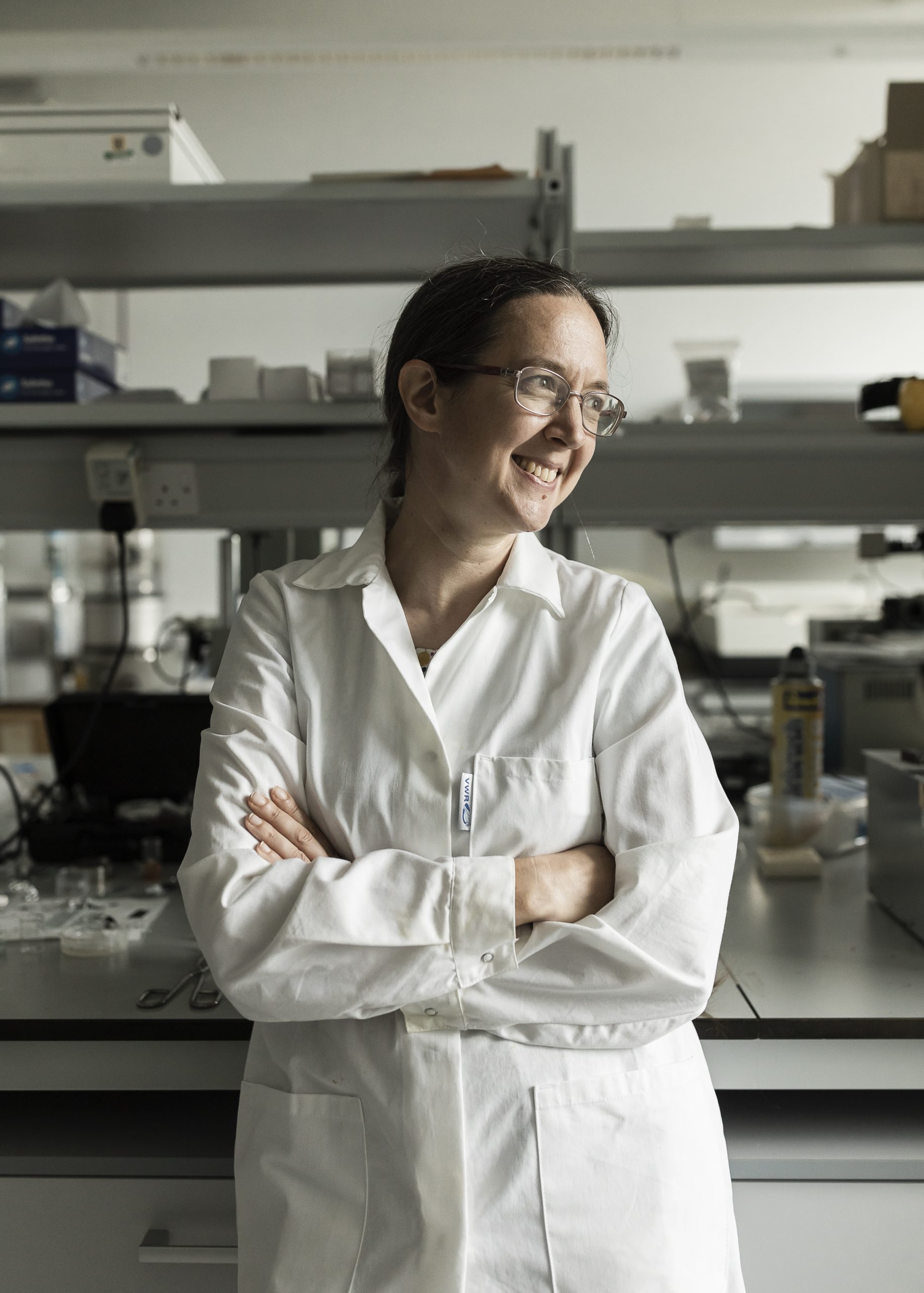
Multi-microscopy investigations of defects in semiconductors
Multi-microscopy (also known as correlative microscopy) is an approach to the nanoscale analysis of the structure and properties of materials in which different microscopy techniques are brought to bear on exactly the same nanoscale structure, revealing more about its characteristics than any individual technique could achieve alone. Here, we focus on the application of scanning probe microscopy (SPM), cathodoluminescence (CL) in the scanning electron microscope (SEM) and transmission electron microscopy (TEM), and the information their coordinated application can provide concerning defects in semiconductor materials. In order to effectively bring these diverse microscopies to bear on exactly the same nanoscale defect, specific protocols and specialist sample preparation techniques have been developed. These will be illustrated via a range of examples of studies of defects in two contrasting families of semiconducting materials: the copper-chalcopyrites and the nitrides. Not only defects that cause degradation of performance in devices (such as grain boundaries in chalcopyrite solar cells) but also defects whose properties can be exploited to achieve new device structures (dislocations in gallium nitride which facilitate the fabrication of porous nitride devices) will be addressed
About the speaker
Rachel Oliver is a materials scientist, inventor and spinout founder, and Director of the Cambridge Centre for Gallium Nitride. Her passion for understanding and engineering the small-scale structure of semiconductor materials to enable new technologies has been recognised in 2021 by her selection as an IEEE Photonics Society Distinguished Lecturer and in 2023 by the award of a Royal Academy of Engineering Chair in Emerging Technologies. Rachel is an advocate for equality, diversity and inclusion in science and engineering, and has addressed the Parliamentary and Scientific Committee on these issues. She is also engaged with policy-making as a member of the Advisory Board to the All Party Parliamentary Group on Semiconductors, and was a member of the UK semiconductor strategy delegation to Washington DC in 2023.
- Onsite at Belval Campus, where you will have the opportunity to meet the speaker over the lunch. A catering is offered only to registered participants at 12.00 at MSA – 3rd floor . Please register before 5 December.
- Online – through Webex – to allow you to listen to the talk in case you are travelling or cannot make it on-site at Belval Campus